| Pin | Symbol | Level | Descripition |
|---|
| 1 | Vss | 0V | Ground |
|---|
| 2 | Vdd | 5.0V | Supply Voltage for Logic |
|---|
| 3 | VO | (variable) | Operating voltage for LCD |
|---|
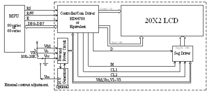
| 4 | RS | H/L | H: DATA, L: Instruction code |
|---|
| 5 | R/W | H/L | H: Read(MPU->Module) L: Write(MPU->Module) |
|---|
| 6 | E | H,H->L | Chip enable signal |
|---|
| 7 | Data 0 | H/L | Data bit 0 |
|---|
| 8 | Data 1 | H/L | Data bit 1 |
|---|
| 9 | Data 2 | H/L | Data bit 2 |
|---|
| 10 | Data 3 | H/L | Data bit 3 |
|---|
| 11 | Data 4 | H/L | Data bit 4 |
|---|
| 12 | Data 5 | H/L | Data bit 5 |
|---|
| 13 | Data 6 | H/L | Data bit 6 |
|---|
| 14 | Data 7 | H/L | Data bit 7 |
|---|
| 15 | A | - | LED+ |
|---|
| 16 | K | - | LED- |
|---|
LCD Character Locations
| Location |
1 |
2 |
3 |
4 |
5 |
6 |
7 |
8 |
9 |
10 |
11 |
12 |
13 |
14 |
15 |
16 |
17 |
18 |
19 |
20 |
Address |
00 |
01 |
02 |
03 |
04 |
05 |
06 |
07 |
08 |
09 |
0A |
0B |
0C |
0D |
0E |
0F |
10 |
11 |
12 |
13 |
Address |
40 |
41 |
42 |
43 |
44 |
45 |
46 |
47 |
48 |
49 |
4A |
4B |
4C |
4D |
4E |
4F |
50 |
51 |
52 |
53 |
Function
The LCD display Module is built in a LSI controller, the controller has two 8-bit registers, an
instruction register (IR) and a data register (DR).
The IR stores instruction codes, such as display clear and cursor shift, and address information for
display data RAM (DDRAM) and character generator (CGRAM). The IR can only be written from
the MPU. The DR temporarily stores data to be written or read from DDRAM or CGRAM. When
address information is written into the IR, then data is stored into the DR from DDRAM or
CGRAM. By the register selector (RS) signal, these two registers can be selected.
| RS | R/W | Operation |
|---|
| 0 | 0 | IR write as an internal operation (display clear, etc.) |
| 0 | 1 | Read busy flag (DB7) and address counter (DB0 to DB7) |
| 1 | 0 | Write data to DDRAM or CGRAM (DR to DDRAM or CGRAM) |
| 1 | 1 | Read data from DDRAM or CGRAM (DDRAM or CGRAM to DR) |